Devices & wafer fabrication
Follow transistor architectures, materials and process steps—from crystal growth and doping to thin films, CVD and ALD.
PTI technical reference · Kindle, paperback & hardcover
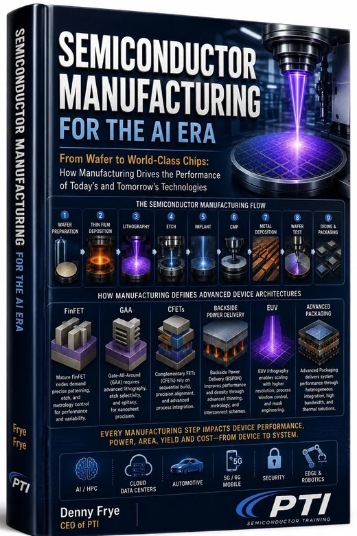
Understand the manufacturing behind AI chips.
Connect device physics, wafer fabrication, advanced packaging and fab operations in one 29-chapter semiconductor manufacturing reference.
Available in Kindle, paperback and hardcover.
See Amazon for format options, current pricing and availability.
Reader perspectives
Comments on Semiconductor Manufacturing for the AI Era from semiconductor industry leaders.
“Semiconductor Manufacturing for the AI Era is fantastic reference text. I had an opportunity to review the book and had trouble putting it down. In fact, my son also looked through it and was equally impressed. This is an outstanding resource for anyone seeking a deeper understanding of semiconductor technology and manufacturing.”
“So far, I have reviewed the first two chapters and I am completely impressed. I intend to review the entire book, well done.”
“Your book is incredibly well written!! And the graphics are great!!!
It's a simple to understand compilation of what it took me 50 years to learn. And now it brings me up to date!!”
“Excellent text book. Unique source for teaching and understanding the Semiconductor Manufacturing Processes in one place. You guys did a great job and created a powerful tool.”
From device to system
A technical reference for semiconductor professionals, advanced students and educators looking beyond a high-level industry overview.
Follow transistor architectures, materials and process steps—from crystal growth and doping to thin films, CVD and ALD.
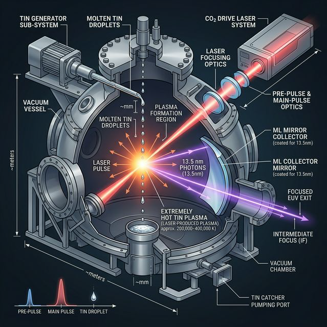
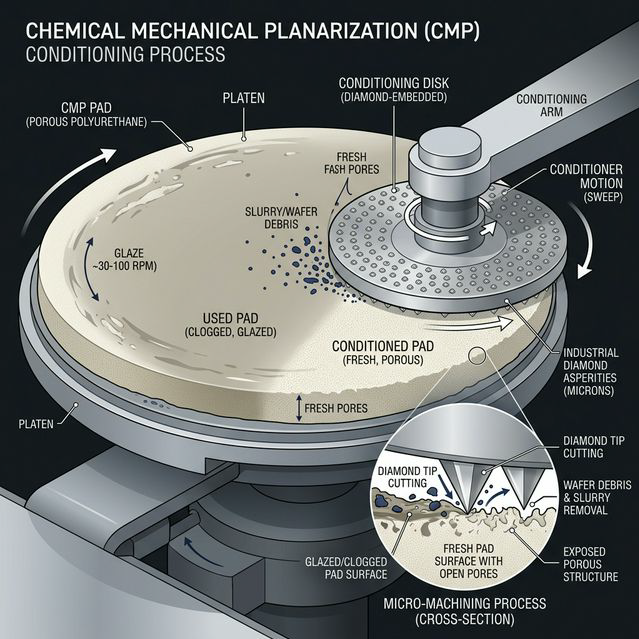
Connect EUV and High-NA lithography with atomic-scale etching, CMP, metallization and interconnect technology.
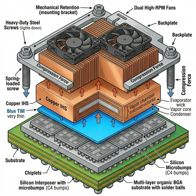
Explore HBM, 3D NAND, hybrid bonding and chiplets alongside yield management, testing, safety and maintenance.
Table of contents
Review the chapter list to see how the book fits your work, studies or training program.
Inside the book
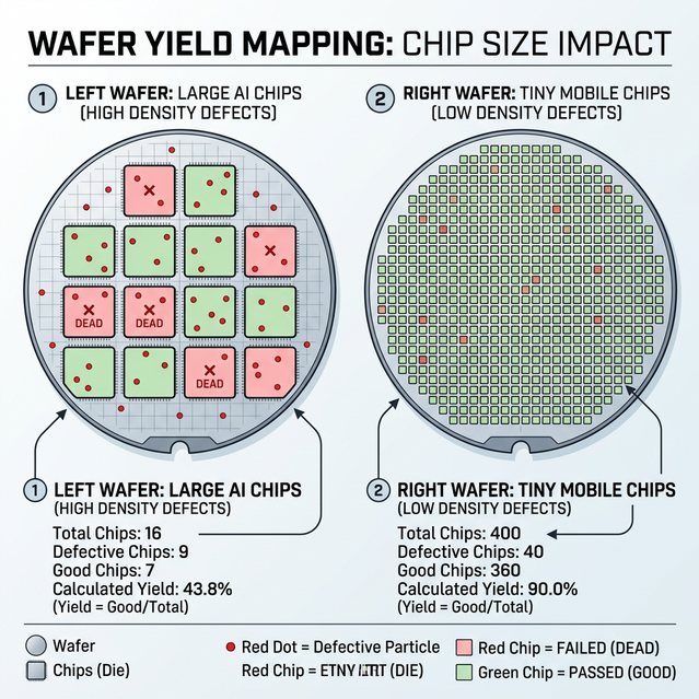
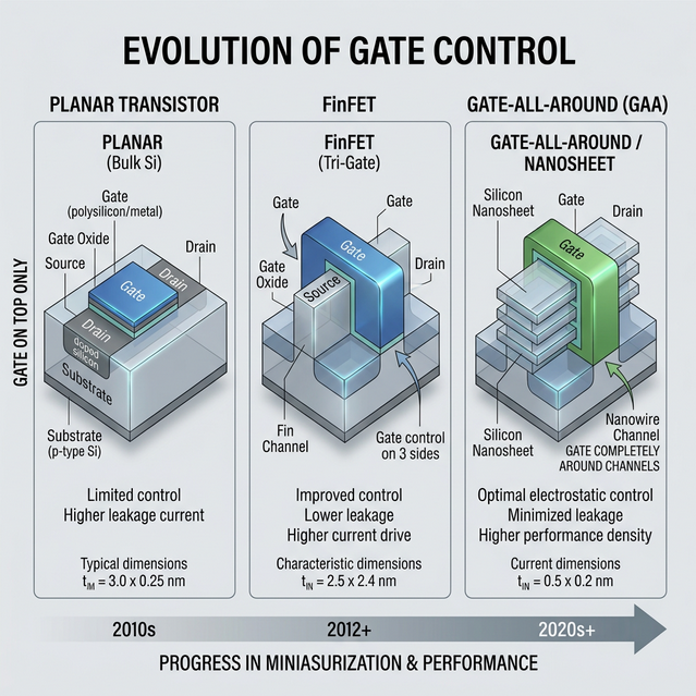
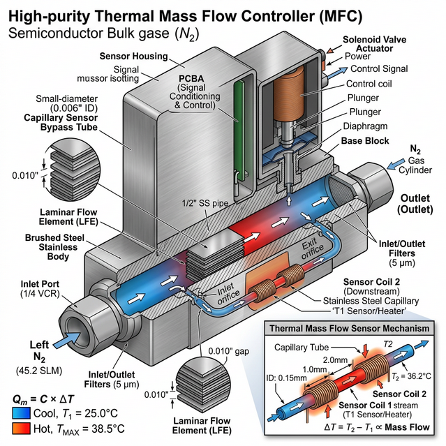
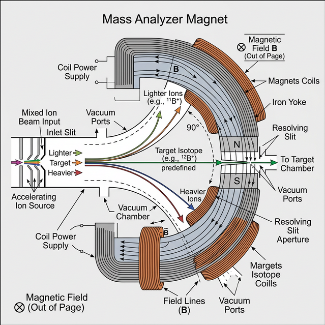
Selected illustrations from the book. Open an image to view it at full size in a new tab.

Meet Denny Frye
Semiconductor Manufacturing for the AI Era brings PT International’s technical training perspective to a semiconductor reference.
Denny Frye brings a practical training perspective to the processes and technologies covered in the book.
Meet Denny and PT InternationalTeaching experience
These comments concern Denny’s teaching, not reviews of this book.
"Denny presented a wonderful semiconductor seminar! He should create a textbook with his knowledge and expertise!"
"He does an excellent job of making complex ideas easy to understand."
"He has an in-depth firsthand as well as academic knowledge of the subject, most of all his teaching/training style is most engaging and very easy to follow regardless of your own background knowledge."
Your semiconductor reference
Choose Kindle, paperback or hardcover on Amazon. Check the listing for current pricing and availability.
View book on Amazon